Products>Multilayer Power Inductors>Technologies

We propose optimal power inductors with our original “material technology”, “process technology”, and “magnetic circuit design technology”.
We offer the products that satisfy customers with advanced ferrite development technology and optimum magnetic circuit design technology.Responding to the needs for "small size and low profile", we will develop products with excellent low loss and high frequency characteristics and contribute to lower power consumption of DC-DC converters.

Core technology ― Create optimal products in a consistent system from material development ―
| Material technology | |
|---|---|
| We develop own unique ferrite materials that match switching frequency of DC-DC converter. We realize products that are optimized to meet customer requirements at the material level. Develop the best material for your requirements We are developing the best ferrite materials that meet customer needs using our original technology. Development of “High-μ” and “High-B” materials for customer requests of compactness and low profile Realization of low hysteresis loss in the high frequency range By developing products from materials, we provide products that satisfy our customers. |
 |
| Magnetic circuit design by CAE technology | |
|---|---|
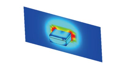
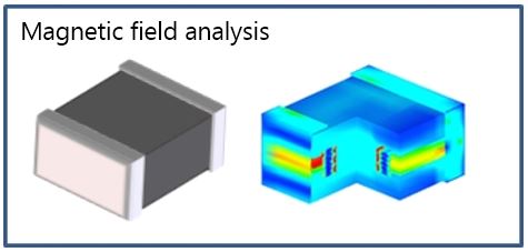
| Total analysis of multilayer power inductors is realized by our original CAE technology. Utilize original magnetic circuit design technology NJ components have our original magnetic circuit design technology by CAE, based on development of ferrite material have cultivated. In multilayer power inductors, the internal conductor and the base magnetic material are sintered together, so it is essential to design and analyze not only magnetic field analysis but also various effects such as internal stress and loss. In addition, spatial magnetic field analysis has been added to cover all items required for multilayer power inductors, and highly accurate simulation design has been realized. |
 |
| Fine printing technology | |
|---|---|
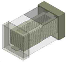
| Fine design is possible using high-precision printing technology. We realize pattern design at the micron order level. Utilize original magnetic circuit design technology The original fine printing technology enables fine pattern design and improves inductor characteristics. By suppressing the magnetic saturation of local magnetic materials, we can realize small and low-profile products. |
 |
Technical topics
| Small size and low profile technology ― Further reduction in size and height of multilayer power inductors ― | |
|---|---|
 |
|
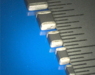
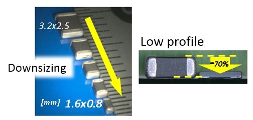
| Created small size and low profile without deterioration of characteristics As the product size becomes smaller and thinner, generally inductor characteristics such as initial inductance and DC bias characteristics are degraded. However we can suppress the deterioration of inductor characteristics to the utmost with our unique ferrite material and design technology, and realize a small size and low profile up to "1005 size" and "height 0.3mm". |
 |
| Optimal magnetic circuit design by magnetic field analysis Multilayer power inductors are electronic components that convert electrical energy into magnetic energy and vice versa. The characteristics of multilayer power inductors greatly affect the characteristics of the voltage conversion circuit, which is the main application, so it is important to realize high-performance products. We use the original CAE technology to optimize the magnetic circuit design and realize small and low profile products with excellent inductor characteristics. |
 |
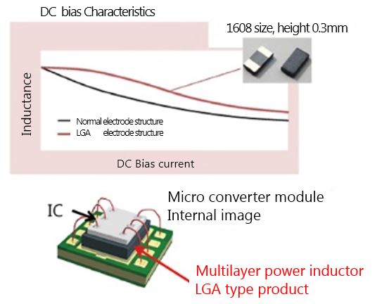
| Lineup of LGA products (one-side terminal products) NJ components have various lineup of LGA products and offer it to customers. Generally, volume of magnetic material affect to electric properties, especially DC bias characteristic. Above all thinner product have more sensitivity to the volume. In case of LGA product, the volume of magnetic material is maximized, we can provide thinner inductor with the best performance. Since LGA products do not have terminal on the top, we offer the best inductor for the CoC structure (Chip on Chip) in which the IC as shown in the right figure is mounted on the top of the inductor. |
 |
| Low power consumption technology | |
|---|---|
 |
|
| Achieves low loss through original material development and CAE technology. Low-loss material technology Utilizing the material technology and firing process technology that we have cultivated so far, we have developed ferrite materials with low hysteresis loss. Appling the material to our product, we provide multilayer power inductors with low loss to customer. |
 |
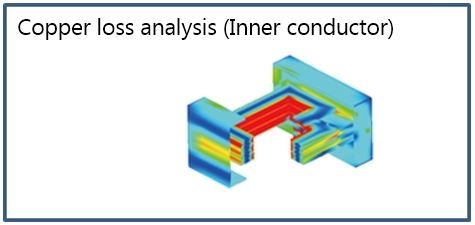
| Utilizing total loss analysis Loss analysis is calculated by subdividing the inductor loss. 1)Analysis of iron loss due to magnetic materials 2)Analysis of copper loss due to conductor Continuous improvement in every detail contributes to realizing the best performance inductor. |
|
| Leakage noise reduction technology | |
|---|---|
 |
|
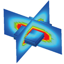
Contributes to stable circuit operation by reducing leakage noise. Spatial magnetic field analysis In an actual power supply circuit, if the noise generated from the inductor interferes with other coils or wiring patterns, the inductance may change or cause wiring noise. We are proceeding with product design that suppresses leakage magnetic flux from the inductor to the outside. |
 |
| Low leakage noise is a strength of multilayer power inductors NJ component multilayer power inductors are chip-formed with high permeability magnetic material, so leakage flux is kept low. 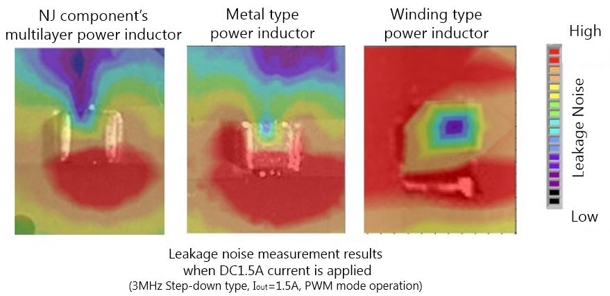 The winding type incorporates a magnetic material in the copper wire part, but the magnetic flux leakage in the winding part becomes very large. Metal power inductors have high magnetic flux leakage due to low magnetic permeability. |
|

