Product Information>Multilayer Power Inductors>Case Studies

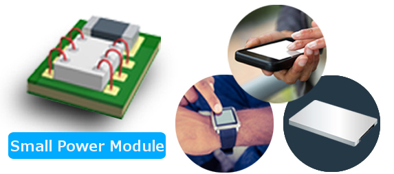
Small power module application ― Achieve even lower power consumption ―
In order to achieve low power consumption and long-term driving of general mobile devices such as FPGA (Field Programmable Gate Array) and smartphone communication PA (Power Amplifier), DC-DC converters that carry voltage conversion function are expensive. Efficiency is required every day.We develop and provide optimal product size design and low loss multilayer power inductors for modules.

| Task | |
|---|---|
| Achieving both compact and low profile and excellent inductor characteristics As power supply modules become smaller, the demand for smaller passive components is increasing. The required characteristics such as current characteristics and frequency characteristics are high, and it was an important development theme to achieve both miniaturization and high performance. |
|
| Our proposal | |
| Optimal magnetic circuit design using simulation We used our own magnetic field analysis simulation to suppress local magnetic saturation.This prevents the core loss from increasing due to magnetic saturation and achieves a compact and excellent power inductor. |
|
| Introduction effect / results | |
| Abundant track record of adoption in various mobile devices It is installed in POL for FPGA, other mobile devices, mainly smartphones, and has abundant delivery results over a wide variety of applications. |
|
|
Representative products MIPSDZ2012G series MIPSBZ3225D series |
Creating multilayer power inductors with a height of 0.35mm or less for smart card / SIM applications
For next-generation smart cards with high security functions, we offer ultra-thin multilayer power inductors with a height of 0.35 mm or less. By adopting an ultra-thin multilayer power inductor, a DC-DC converter can be mounted inside the card.| Task | |
|---|---|
| Low profile and high inductance There was a height limit of 0.4mm or less to fit in the card, and a high inductance value was required even though the number of turns of the inner conductor was limited. |
|
| Our proposal | |
| Application of printing lamination technology and LGA technology By using the printing lamination technology that we have cultivated so far, we can achieve fine patterns per layer. In addition, the LGA electrode structure was used to maximize the volume of the magnetic material and meet customer needs. |
|
| Introduction effect / results | |
| Adoption to smart card manufacturers We have a track record of delivery to the latest smart cards equipped with Bluetooth and fingerprint authentication functions. |
|
|
Representative products MIPSKZ1608G series |
Achieve high efficiency for wearable devices
Communication performance and low power consumption are indispensable to achieve wearable devices that can be connected anywhere and anytime.Especially for small devices, the battery capacity is small, and high efficiency is required for the power supply installed inside.
We are responding by creating "shape and characteristics" in line with customer requests.

| Task | |
|---|---|
| Minimizing standby power consumption To achieve long-time operation for devices that can only be equipped with small batteries, it is necessary to minimize power consumption, especially during standby. In addition, there is an increasing demand for smaller product sizes for use in circuits. |
|
| Our proposal | |
| Responding to customer needs by developing low-loss magnetic materials By developing and applying low AC loss materials, we provide ultra-compact products that lead to higher power efficiency. |
|
| Introduction effect / results | |
| Achieve high efficiency Achieved high efficiency in DC / DC converters. * 1608 products (Comparison with our company) |
 |
|
Representative products MIPSUZ1608G series |
|

